Date Completed: April 10, 2003
This circuit is an improved version of classical QPSK modulator/demodulator designs in terms of costs. Based on common CMOS logic, it needs no frequency or phase adjustments.
The implementations of the modulator/demodulator circuits are depicted using the following schematic diagrams:
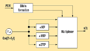
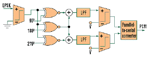
The original design idea and descriptions are published by Eduard Bertran at www.elecdesign.com.
I have implemented the circuit with minor changes from the suggested one. The changes are in dibit formation section in the modulator and also elimination of the phase-references generator due to the fact that in this experiment necessary synchronization for coherent detection is provided by using the same signal generator and although this is not a practical approach but it is sufficient for the cause of this simple experiment which was observing the QPSK modulated signal and also the demodulated PCM signal.
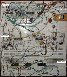
The circuit has been put together in a not-so-neat fashion:
In QPSK modulation, the bit stream of the signal to be transmitted (PCM signal) is sampled first and decomposed into two binary waves (dibits). Each pair of dibits is associated with one of four possible phases of the QPSK modulation. The modulated signal is:
s(t) = Ikcos(2πfct) + Qksin(2πfct)
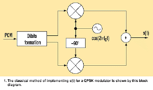
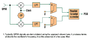
where I and Q are the in-phase and in-quadrature components of the modulated signal. The signal values (1 or −1) determine four points (or symbols) in the QPSK signal space (or constellation). I and Q values are assigned according to associated dibits combinations. The classical circuitry to implement s(t) is based on the block diagram shown in Figure 1.
Higher Resolution
Figure 1
If I and Q take their values from the set [1,−1], the constellation shows four points at phases 45º, 135º, 225º, and 315º. In this case, the QPSK is also called 4-QAM.
The low-cost realization of this circuit consists of rotating the angles of the QPSK constellation by 135º, by increasing the set of possible values of I and Q components to [−1,0,1]. In this case, the table shows the modified phase distribution.
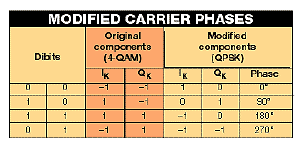
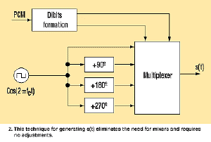
These phases are easily realizable with conventional logic circuitry because the initial phase of 0º is the same as the carrier wave. The remaining phases may be obtained from simple 90º consecutive phase shifts, avoiding the mixers of Figure 1. But that comes only with a slight reduction of the signal-to-noise ratio (Fig. 2).
Higher Resolution
Figure 2
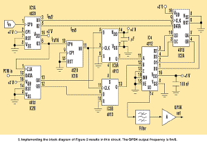
Figure 3 is the actual circuit realization of the block diagram in Figure 2. From a main oscillator of frequency (fm), a frequency divider (IC1A) supplies values of fm/2, fm/8, and fm/16. Acceptable values of fm depend on the selected CMOS technology.
Higher Resolution
Figure 3
Dibits are formed from a digital input (PCM signal) in shift register IC2B, and in the dual flip-flop IC3. The different phases of 0º, 90º, 180º, and 270º are produced at outputs QA, QB, QC, and QD of the four-bit shift register, IC2A.
Finally, the dibits (on pins A and B of IC4) control the multiplexer (data selector) output. This is a selected phase from D0, D1, D2, or D3, according to the dibit combinations. The rest of the circuit is a simple band-pass filter that eliminates DC levels and shapes the pulse, plus an amplifier to set the desired output level. The QPSK output frequency is fm/8.
This demodulator is suitable for the QPSK modulator described in the previous section. Also based on common CMOS logic, it requires no adjustments. The typical approach to QPSK demodulation is the decomposition of the modulated input signal via two multipliers driven by a fixed-frequency oscillator whose two outputs are 90° apart (Fig. 4).
Higher Resolution
Figure 4
This operation also produces terms at twice the rate of the oscillator. So, two low-pass filters (LPFs) are added to eliminate them. Finally, a parallel-to-serial converter translates the dibits to bits, thus producing the desired PCM signal.
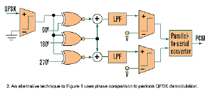
An alternative demodulator that’s suitable for the aforementioned QPSK modulator generates four modified carrier phases (0°, 90°, 180°, and 270°) obtained in the modulator by rotating the angles of the QPSK constellation. Then, a simple XNOR operation between each phase and the modulated signal will produce a logic “1” only if both coincide (Fig. 5).
Higher Resolution
Figure 5
If the received phase is 0° (related to dibit 00), all XNORs produce a logic “0.” If the phase is 90° (dibit 10), only the upper branch gives a “1.” This situation is inverted for 270° (dibit 01). In this case, the logic “1” is produced at the lower branch. But if the phase is 180° (dibit 11), a logic “1” is added to both branches. The result is the demodulated PCM signal.
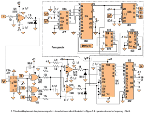
In a practical circuit, the phase-references generator produces inputs to the XNOR gates (Fig. 6).
Higher Resolution
Figure 6
Also, the input, called ERROR (UART), adapts the initial phase reference. This circuit forms a closed loop between the PCM signal and ERROR (UART) that provides the necessary synchronization for coherent detection. Like the modulator, this circuit runs for a carrier frequency of fm/8. It has been tested at 2 MHz (with basic CMOS logic) and at 20 MHz (with HCMOS).